
Test 400 A pulsed current without destroying your socket
Short-circuit, avalanche, and full-output tests push hundreds of amps through a test contactor. Our Ansys-simulated copper Power Block contactor carries the load at about 1/10,000th the current density of a probe-only socket.
Power Block vs. probe-only socket at 400 A
Same device, same current, same 150 °C test cell. The only difference is where the current flows: through a large copper block, or through a handful of spring-probe tips.
| Condition | Contact architecture | Max current density | Thermal outcome | Verdict |
|---|---|---|---|---|
| 400 A continuous full contact | Power Block | 3.2×10⁹ A/m² | +0.5 °C above ambient | Survives |
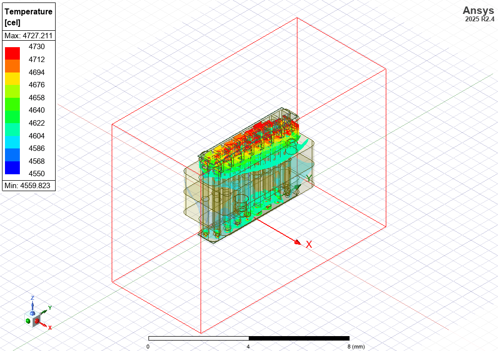
| 400 A continuous full contact | Probe-only (PEEK 450G) | 3.6×10¹³ A/m² | Runaway heating; probe, housing and PCB damage | Destructive |
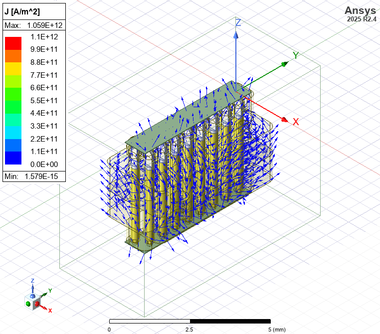
| 400 A, 10 µs pulse full contact | Power Block | ≈2.7×10⁹ A/m² | Stays at ambient | Survives |
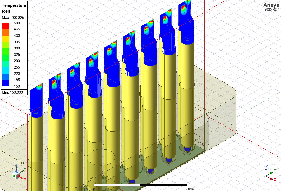
| 400 A, 10 µs pulse full contact | Probe-only (PEEK 450G) | ≈1.1×10¹² A/m² | Probe tips reach 400–800 °C locally | Wears quickly |
| 400 A continuous 0.05 mm gap | Power Block, device not seated | 3.26×10¹³ A/m² | Same runaway as probe-only | Benefit lost |
| 400 A, 10 µs pulse 0.05 mm gap | Power Block, device not seated | Tip-dominated | Probe tips at 500–700 °C; contact resistance rises over life | Degrades |
The device lands on copper, not on probe tips
A gold-plated thermal-copper Power Block sits in direct contact with the device pad. The copper carries the bulk of the current and acts as a heat sink. The spring probes only provide compliance for planarity, so the contact behaves like a device soldered to the PCB rather than a point-contact socket.

Simulation evidence
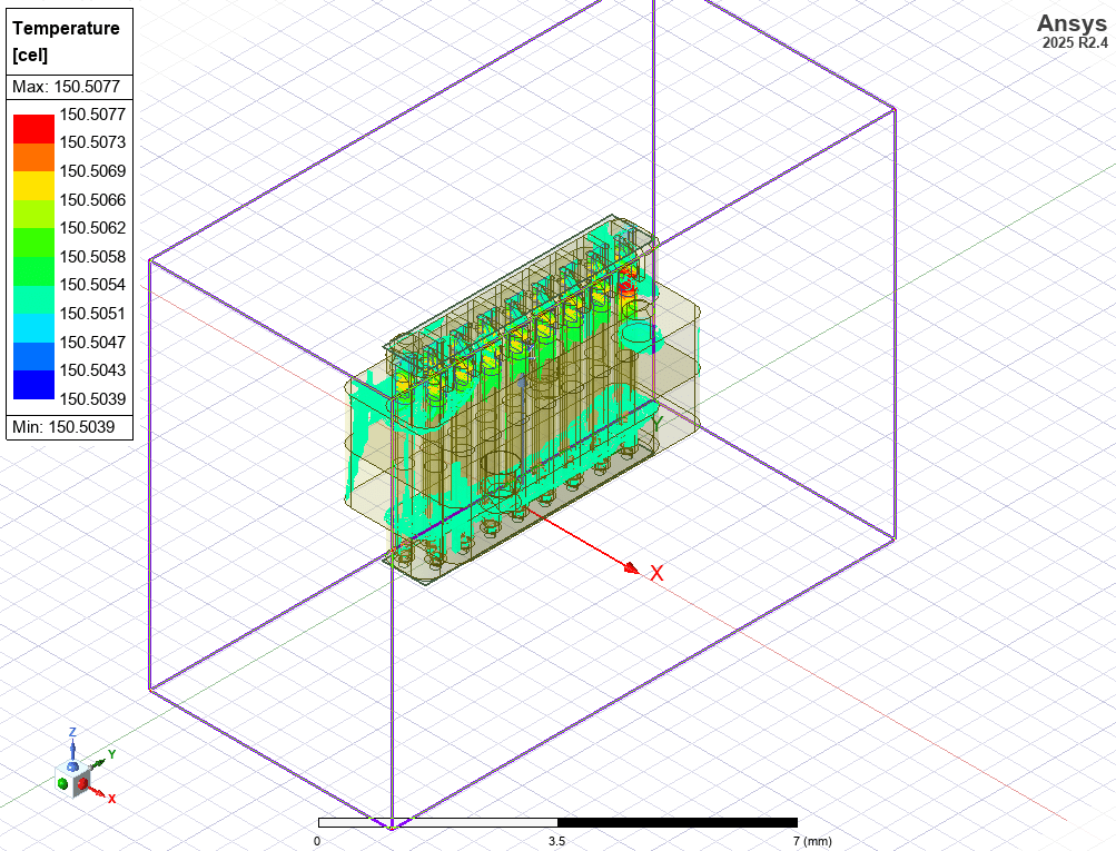
Power Block
3.2×10⁹ A/m² and a 0.5 °C rise at 400 A continuous.Probe-only PEEK socket
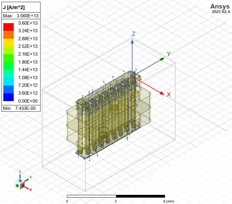
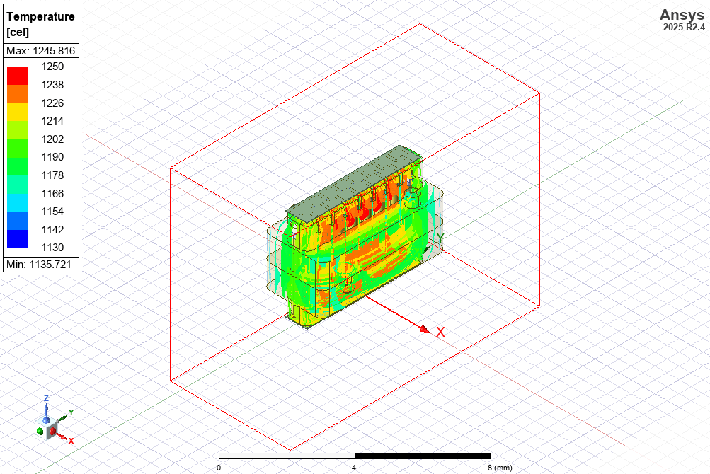
3.6×10¹³ A/m² and runaway heating that damages probes, housing and PCB.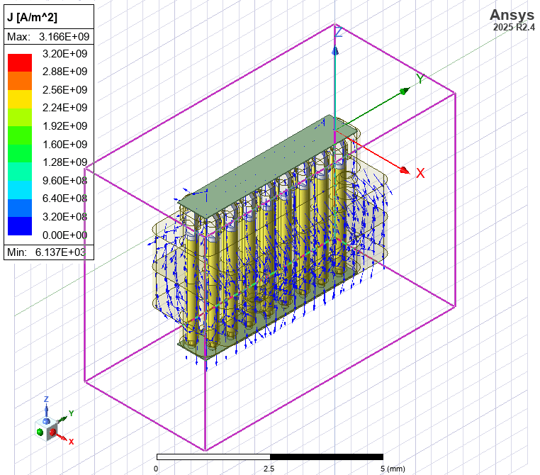
Power Block
About 2.7×10⁹ A/m² for a 10 µs pulse; the assembly stays at ambient.Probe-only PEEK socket
About 1.1×10¹² A/m²; probe tips reach several hundred °C and wear out quickly.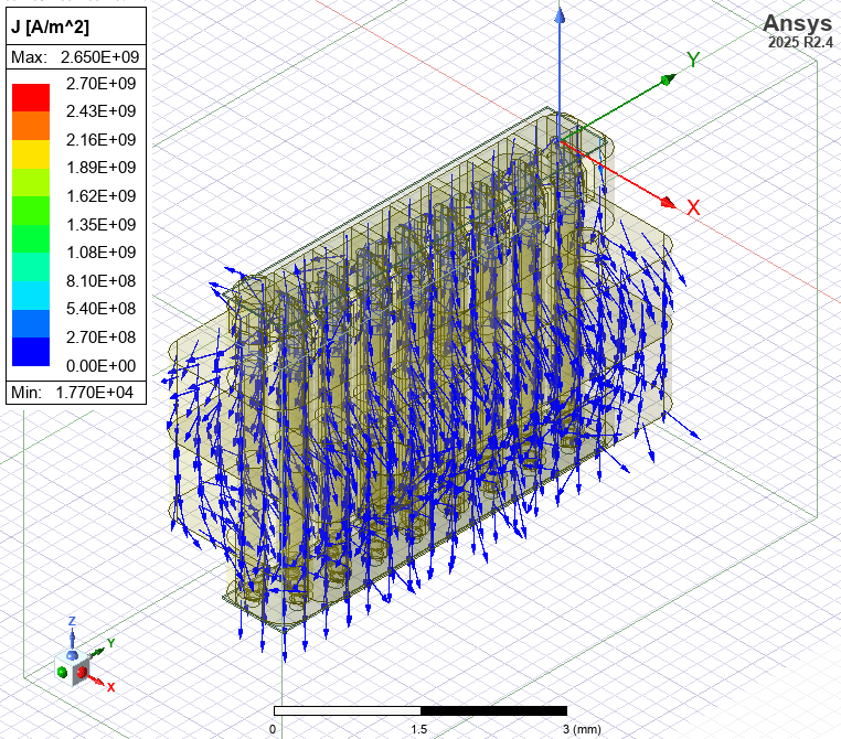


The lesson
The Power Block only works when the device actually seats on the copper.With a 0.05 mm gap
All current flows through the probe tips: 3.26×10¹³ A/m², matching the failed PEEK case.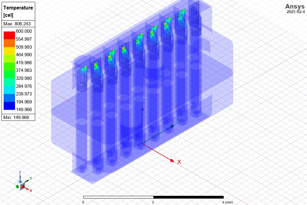
Built for very high current test
Verified performance and the one thing to control
We simulate. We don’t guess.
Current density, power loss, and temperature are simulated for continuous and pulsed 400 A, with and without full contact.
A 0.05 mm gap defeats the benefit
Handler plunger setting, placement, debris, and device thickness or planarity all affect seating. We help you specify and verify it.
Read the full study
Method, boundary conditions, and all simulation figures. Request the complete note from our engineering team.
Technical librarySpec checklist for any high-current socket
- Copper current pathIs the bulk current carried by a copper block, with probes used for compliance?
- Contact resistanceIs bulk resistance published, in the micro-ohm range?
- Pulse thermal analysisHas the vendor simulated your pulse width and duty cycle?
- Seating-height controlHow are plunger setting and planarity controlled?
- Kelvin and sense optionsDo you need dual sense pins on Vin and Vout?
Common questions
Can spring probes alone carry 400 A?
Not safely. In simulation, 400 A continuous through probe tips in a PEEK 450G socket produced a peak current density of 3.6×10¹³ A/m², roughly 10,000× the Power Block case, with runaway heating that damages probes, the housing, and the PCB.
A short pulse is more forgiving, but local tip temperatures still reached several hundred °C in simulation, which shortens socket life.
What is a Power Block contactor?
A gold-plated thermal-copper block that the device pad contacts directly. The copper carries the bulk of the current and acts as a heat sink. The spring probes only provide compliance for planarity.
The result behaves like a device soldered to the PCB rather than a point-contact socket.
How much lower is the current density with a Power Block?
- Continuous 400 A: 3.2×10⁹ A/m² (Power Block) vs. 3.6×10¹³ A/m² (probe-only), about 10,000×.
- 10 µs pulse: about 2.7×10⁹ vs. 1.1×10¹² A/m², about 400×.
Does a 10 µs pulse make a probe-only socket safe?
It helps, but it is not safe for long-term use. A 10 µs, 400 A pulse in a probe-only PEEK socket still produced about 1.1×10¹² A/m² and probe-tip temperatures of several hundred °C (400–800 °C locally). Tips wear and the precious-metal plating migrates, so contact resistance climbs.
With a Power Block, the same pulse leaves the assembly at ambient temperature.
What happens if the device does not seat on the Power Block?
The benefit is lost. With a 0.05 mm gap, all current flows through the probe tips: current density rises to 3.26×10¹³ A/m² and the thermal result matches the failed probe-only case.
Causes include handler plunger setting, placement error, debris, and device thickness or planarity variation. Specify and verify seating with the socket.
What is the resistance and inductance of the Power Block?
- Bulk resistance: 13.7 µΩ
- DC inductance: 806 pH (698 pH at 200 kHz)
- Capacitance: 444 fF
Values were extracted with Ansys Q3D.
How many pins share the current?
The study spreads 400 A over at least 8 pins each for Vin and Vout, at 0.5 mm and 0.45 mm pitch. Other pins carry 500 mA.
What test temperature was simulated?
The test cell was 150 °C. At 400 A continuous with full contact, the Power Block assembly rose only 0.5 °C above that. For a 10 µs pulse it stayed at ambient.
Is this suitable for short-circuit and avalanche testing?
Yes. With solid contact between the device and the Power Block, the simulations support short-circuit, avalanche, and full-output functional tests, and project insertion counts in the hundreds of thousands. The key requirement is controlled device seating.
Does this apply to a 300 A DC-DC converter test?
The simulations cover 400 A. Current density scales with current, so a 300 A test sits in a less severe regime, and the same architecture and seating requirements apply. For a specific device, share your pulse width, duty cycle, and pin map with our engineers for a dedicated simulation.
Which handler and tester were used?
The socket was designed for an MT9510 handler and ETS364 tester, with a manual actuator that supports a thermocouple.
Does it support Kelvin sensing?
Vin and Vout use a single port with dual sense pins (no Kelvin on the power pins in this design). Other signal pins support Kelvin connections.
What is the Power Block made of?
Thermal copper, gold plated, with a proprietary precious-metal alloy contact surface. The comparison case used probes in a PEEK 450G housing.
Does this apply to bare die, strip, or wafer testing?
The published study covers a packaged power device with a SW-bus pad contacted by the Power Block. Bare die, strip, and wafer formats are not part of this study. If you test in those formats, send us your current profile and contact geometry and our engineers will advise.
What should I include in a quote request?
- Peak current, pulse width, duty cycle
- Package dimensions, POD, and pad interconnect type
- Number of Vin/Vout pins sharing current
- Test cell temperature and handler type
- Kelvin or sense requirements